Milling a PCB with Auto-Leveling using a Carbide 3D Nomad 3
I tried Carbide Copper, which looks abandoned and did not spin the spindle for me. I also tried FlatCAM and bCNC, and bricked my Nomad 3 with bCNC. With help from Carbide 3D support, I wrote instructions to reset GRBL on a Nomad 3.
I settled on pcb2gcode to generate G-code and coppercli to run the mill.
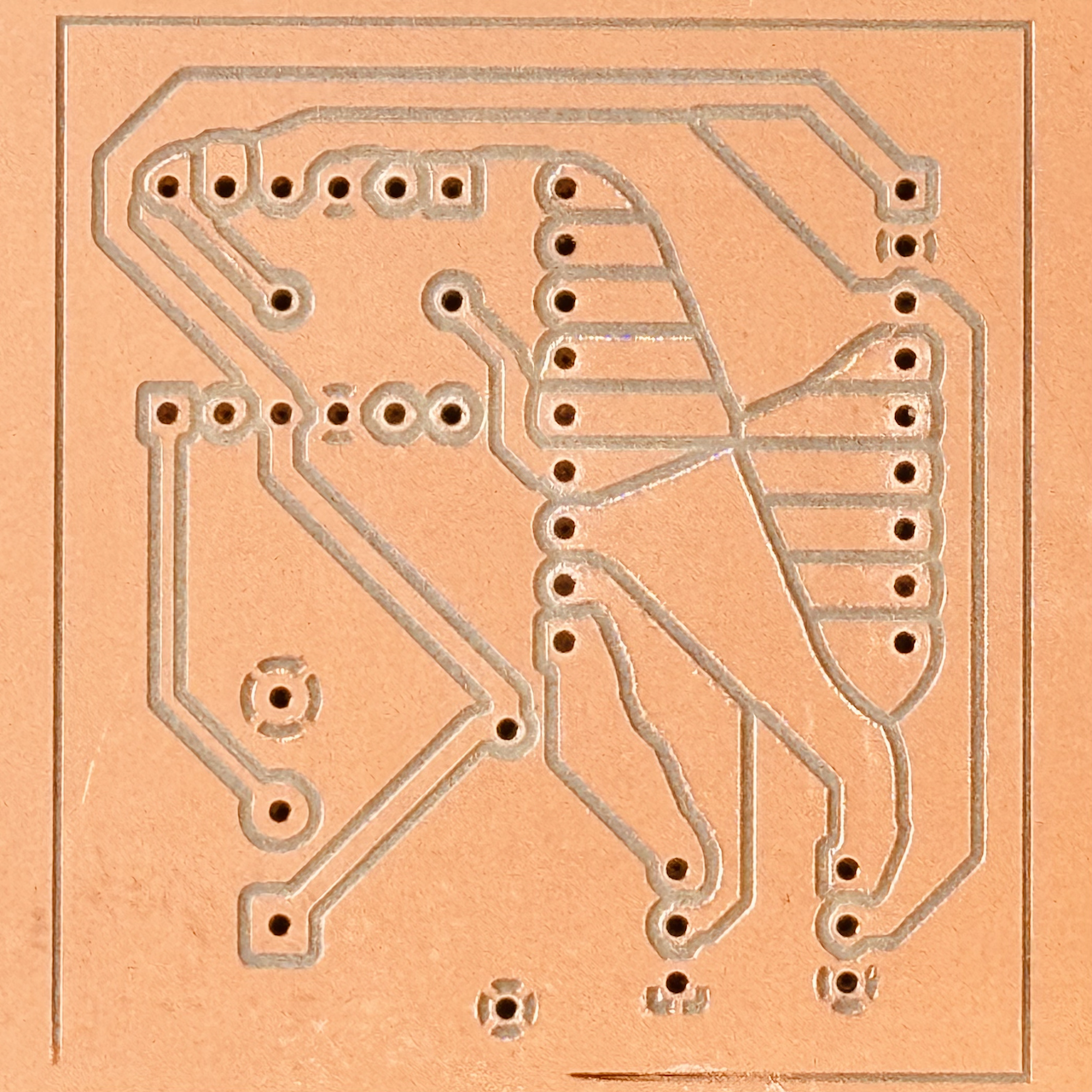
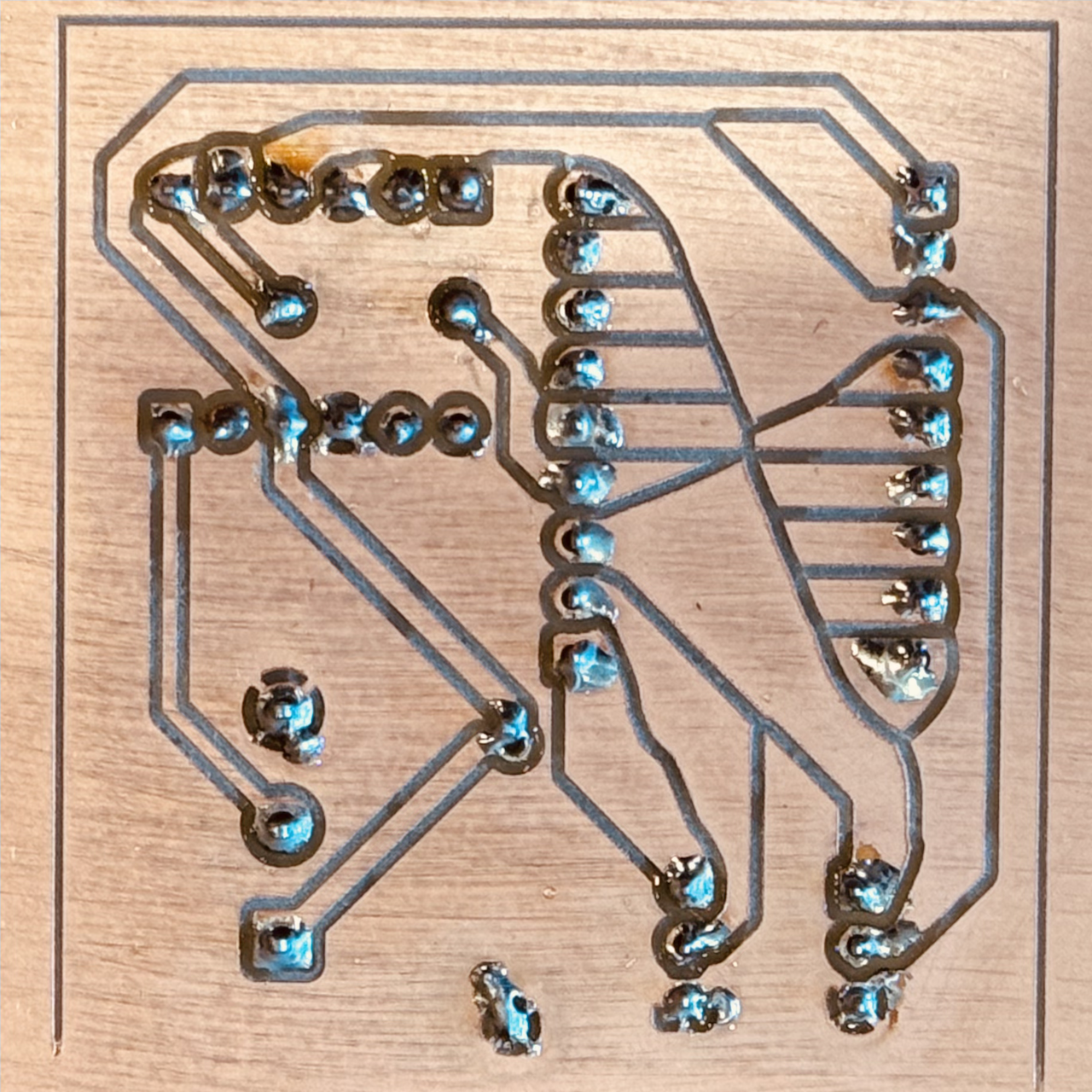
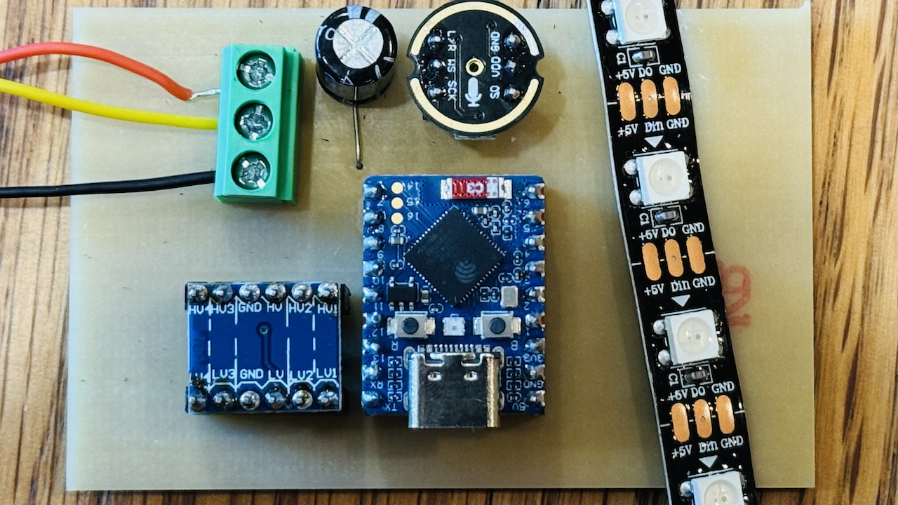
Example Results
Video: Probing
Acknowledgments
Chris Kohlhardt's notes partly inspired this work. He uses FlatCAM and bCNC, which I found hard to use. Thanks to Martin Pittermann for OpenCNCPilot, which coppercli is based on, and for the feedback. Thanks to deHarro for tutorial feedback. Thanks to Eyal for pcb2gcode.
CNC Machine
I tested this on a Carbide 3D Nomad 3.
 coppercli
coppercli is a cross-platform (Mac, Linux, Windows, and web) tool for PCB milling on GRBL machines with probe-based auto-leveling, tool changes, real-time visualization, depth-adjusted remills, and session recovery. It is based on OpenCNCPilot.
- Runs directly over USB/serial as a keyboard-driven terminal app
- Runs as a USB/serial proxy, so a terminal on another computer on your network can control the machine
- Runs as an HTTP server, so you can control the machine from a browser (desktop or mobile)
PCB Blanks / Copper Clad
Use only FR1 copper clad. Never mill FR4 in a CNC machine: FR4 is glass fiber, and milling it makes glass dust that damages your lungs.
I use 2x3" and 4x6" PCB blanks from Carbide 3D, and have also used 100x150mm and 150x200mm blanks. Blanks are single-sided ("SS") or double-sided ("DS"); Amazon and AliExpress sell them too. Buy FR1, never FR4.
If you put the components on the bare side and solder their pins on the copper side, as this tutorial does, you need single-sided copper clad.
A ground plane on the other side needs double-sided copper clad, and I have not yet found a good way to work with it. A pin pushed through double-sided clad will likely touch the copper on both sides of the board, even if you solder only one side.
V-Bits
Where I buy 30°, 40°, and 60° V-bits.
30° V-bits
- #501 PCB Engraver (30°) bits from Carbide 3D
- Coated 30° V-Groove bits from bits&bits
- FoxAlien 30° bits via Amazon are my favorites because they are cheap and work well.
40° V-bits
60° V-bits
Jigs
I published jigs in several sizes on printables.com. Contact me if you need another size. If you do not have a 3D printer, I can print them and send them to you for $49.99 plus shipping; others can do it for much less.
Rig the BitZero
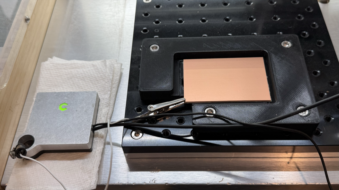
Connect the ground of the BitZero V2 to the top of the copper clad. Any conductor works. My rig uses an alligator clip on the copper clad:
Workflow Outline
- Adjust the PCB design.
- Export Gerber files.
- Generate G-code with pcb2gcode.
- Attach the copper clad to the jig with double-sided tape.
- Zero X, Y, Z.
- Probe to create a height map. This takes 15-30 minutes, depending on board size and grid size.
- Mill the traces (for example, with a 30° V-bit). This takes 30 minutes to 3 hours, depending on the board.
- [Optional: flip, mill other side, flip back]
- Replace V-bit with a drill bit (for example, a 0.8mm PCB drill).
- Zero Z.
- Drill holes.
- Cut the outline.
- Sand and clean the copper.
- Solder.
If you mill both sides, drill after milling both sides; otherwise you probe a surface with holes in it.
Single-layer Design on B.Cu
This tutorial makes a single-layer PCB: you plug in components at the top and solder them at the bottom, so your entire PCB design must be on B.Cu.
If you first designed your board for a PCB fab (e.g., JLCPCB, PCBWay, OSH Park), you likely put the GND plane on B.Cu and the signal traces on F.Cu. That does not work for CNC milling. (I discovered this the hard way when all my pin holes were mirrored.)
To adapt the design, move all routing, including GND, to F.Cu. Without the GND plane, you will likely have to reroute traces.
Also widen the tracks and the clearance:

Using File → Board Setup → Design Rules → Net Classes:
- Set Clearance to 0.34mm for all net classes; larger values caused problems for me.
- Set Track Width to a minimum of 0.6mm for all net classes; I go up to 1mm for higher-voltage classes.
- Set Via Size to 0.6mm.
- Set Via Hole to 0.3mm.
- Set µVia Size to 0.3mm.
- Set µVia Hole to 0.1mm.
- Set DP Width to 0.4mm.
- Set DP Gap to 0.5mm.
Using File → Board Setup → Board Stackup → Physical Stackup:
- Set Copper layers to 2 using the drop-down at the top of the window.
To apply the new net class values to existing tracks, use Edit → Edit Track and Via Properties, select Set to net class / custom rule values, and press Apply. Then run the Design Rules Checker and fix the errors the wider tracks cause. Other people report using thinner tracks.
Once everything is on F.Cu, swap F.Cu and B.Cu with Edit → Swap Layers.... If you will not send the board to a fab, route everything on B.Cu from the start.
Check Your PCB
My most frequent mistakes are rotated pin headers and misaligned pins. To catch them:
- Hold the parts against the screen, next to the layout.
- Check pin assignments.
- Check pin spacing (typically multiples of 2.54mm) and alignment with KiCad's measuring tool, or align the pins automatically with the Snap To Grid function in the
pcb-action-toolsplugin. - Measure the physical pins with a caliper and compare them with the layout.
- Run DRC and fix all violations and unconnected items.
KiCad PCB Export
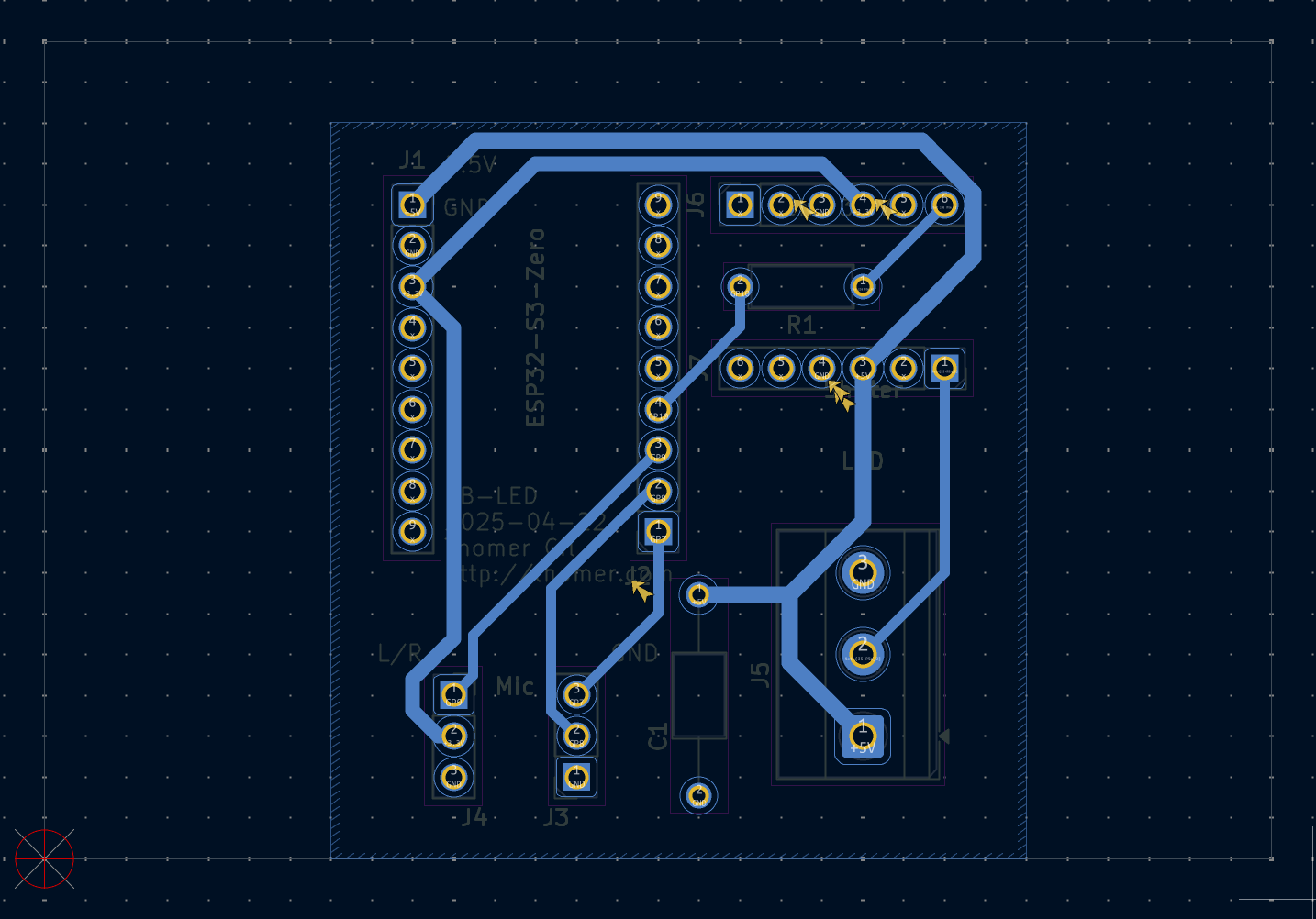
Before exporting from KiCad's PCB editor:
- The CNC cuts the board out of the copper clad along the Edge.Cuts layer.
- Leave at least 2mm between the board edge and the circuitry.
- With Place → Drill/Place File Origin, put the drill/place file origin at the bottom left of the Edge.Cuts outline.
- With Place → Grid Origin, put the grid origin at the same point.
KiCad Plot / Export
Using menu File → Plot...:
- ☑ F.Cu
- ☑ B.Cu
- ☑ Edge.Cuts
- ☑ Use drill/place file origin
- ☐ Use extended X2 format (leave unchecked)
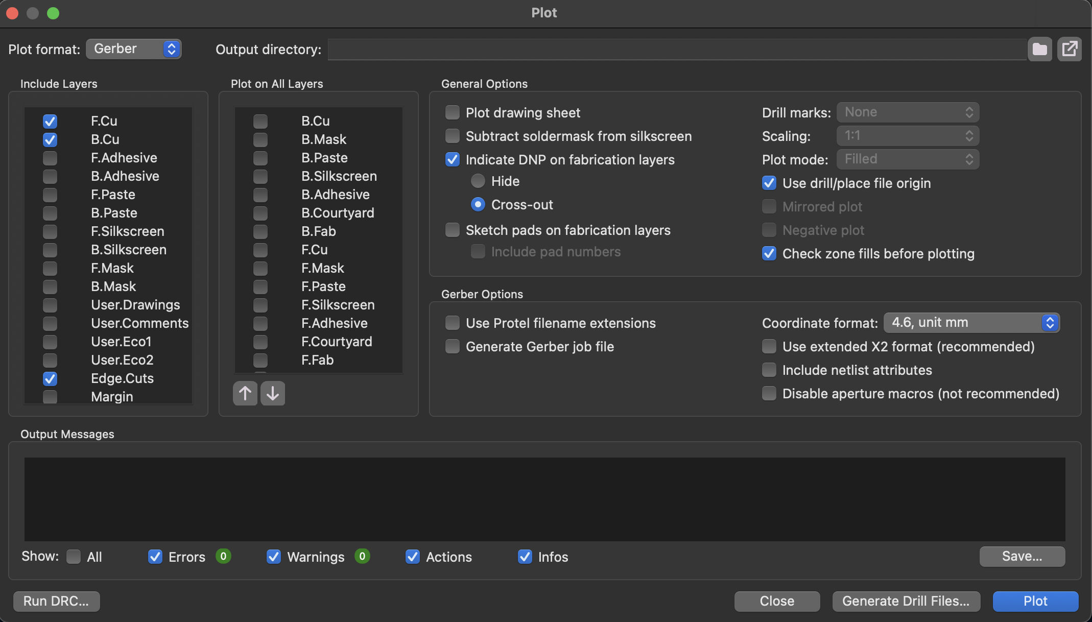
Press "Plot".
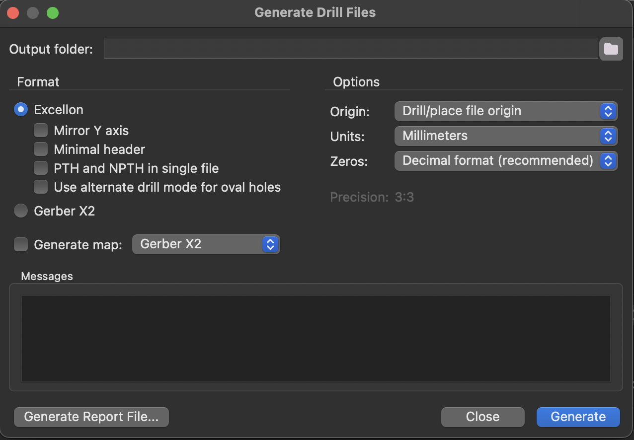
Then press Generate Drill Files... and set:
- Excellon format
- Origin: Drill/place file origin
- Units: millimeters
- Zeros: decimal format (recommended)
Then press "Generate".
Back on the Plot window, press "Plot".
Generate G-code from .gbr Files
Using pcb2gcode and the millproject configuration file.
Create a file millproject in the same directory as the .gbr files.
# See https://github.com/pcb2gcode/pcb2gcode/wiki/Manual

metric=true
metricoutput=true

# milling
zwork=-0.10          # Depth in mm; depends on your V-bit
zsafe=20             # Height for movements; start with 20mm, can be 1mm if confident
# zsafe=1            # What I use
zchange=35           # Height for tool changes
mill-feed=600        # Feed rate in mm/minute; lower it if cuts come out rough
mill-speed=12000     # RPM for milling
nom6=1               # Suppress tool changes; pcb2gcode-wrapper --multi handles them
spinup-time=3.0      # Time to spin up the spindle in seconds
spindown-time=3.0    # Time to spin down the spindle in seconds
backtrack=1          # Retrace milled paths when faster than lifting
isolation-width=0.3  # Widest isolation that works for me
milling-overlap=25%  # Overlap between the passes that widen the isolation

# Voronoi regions
voronoi=1            # Leaves more copper for easier soldering, but looks odd; default 0
# min-path-length=0.1 # Removes tiny Voronoi artifacts; in a pending pull request

# drilling
zdrill=-1.7          # Drill depth; measure your copper clad
zmilldrill=-1.7      # Mill drill depth; measure your copper clad
drill-feed=200       # Feed rate in mm/minute
drill-speed=14000    # RPM for drilling
nog81=1              # Use G0/G1 instead of G81/G80; required for coppercli
drills-available=0.8 # Your 0.8mm drill bit
min-milldrill-hole-diameter=0.81 # Milldrill holes larger than the 0.8mm drill bit
milldrill-diameter=0.8 # Same drill bit as drilling

# outline cutting
zcut=-1.7            # Cut depth for outline; same as drill depth
cut-feed=200         # Feed rate for outline cutting
cut-vertfeed=200     # Vertical feed rate
cut-speed=16000      # RPM for cutting
cutter-diameter=0.8  # Diameter of end mill for cutting (in mm)
bridgesnum=0         # No bridges; tape holds the board
cut-infeed=0.4       # Max cutting depth per pass

# Conflicts with --x-offset and --y-offset; do not use
# zero-start=true
Check these values before you mill:
zsafeis the travel height of the bit. If it is too low, the bit crashes into the jig and breaks. Once you trust your setup, you can lower it to 1.zchangeis the height for changing bits. If it is too high and the bit is long, the machine hits its Z hard limit and the job stops with an error.zworkis how deep the mill cuts into the copper clad. I start at-0.10with a 30° V-bit; the right depth depends on your V-bit.nom6=1leaves tool change commands out of the individual files;pcb2gcode-wrapper --multiadds them when it combines the files.nog81=1stopspcb2gcodefrom writingG81drill cycles, which coppercli does not support.--mill-diameters, passed on the command line below, is the width the V-bit cuts atzwork. This tool cutting width calculator computes it. For a 30° V-bit with a 0.1mm tip atzwork=-0.10, it is 0.1 + 2 × 0.10 × tan(15°) ≈ 0.15.- The feeds and speeds above are what I use. If cuts come out rough, lower
mill-feedanddrill-feed.
Run pcb2gcode to generate the back, (B.Cu), which is the side we mill.
# replace "decibel-meter-B_Cu.gbr" with your own .B_Cu file
# optional: --basename FOO to prefix the output file names
# optional: --output-dir DIR to write the output to another directory
# optional: --x-offset negative number moves the PCB to the right of the origin
#           this should equal the width of your board
# --mill-diameters: the width the V-bit cuts at zwork
pcb2gcode --back decibel-meter-B_Cu.gbr --mill-diameters=0.15
Generate the Excellon drill file:
# replace "decibel-meter-PTH.drl" with your own .drl file
# optional: --basename FOO to prefix the output file names
# optional: --output-dir DIR to write the output to another directory
# optional: --x-offset negative number moves the PCB to the right of the origin
#           this should equal the width of your board
#           must match the --x-offset used for B_Cu above
pcb2gcode --drill decibel-meter-PTH.drl --drill-side back
Generate the outline file:
# replace "decibel-meter-Edge_Cuts.gbr" with your own .Edge_Cuts file
# optional: --basename FOO to prefix the output file names
# optional: --output-dir DIR to write the output to another directory
# optional: --x-offset negative number moves the PCB to the right of the origin
#           this should equal the width of your board
#           must match the --x-offset used for B_Cu above
pcb2gcode --outline decibel-meter-Edge_Cuts.gbr --cut-side back
Alternatively, install my pcb2gcode-tools package:
brew install pipx
pipx install git+https://github.com/thomergil/pcb2gcode-tools
Then run pcb2gcode-wrapper. It runs the three pcb2gcode commands above with the same options, calculates the offsets from your Edge_Cuts.gbr file, and post-processes the output:
$ pcb2gcode-wrapper decibel-meter --mill-diameters=0.15It sets --x-offset to -1 * (ceil(width_mm) + x_margin) and --y-offset to y_margin. x_margin defaults to 5mm and y_margin to 3mm. To change them:
$ pcb2gcode-wrapper decibel-meter --mill-diameters=0.15 --x-margin 10 --y-margin 7The wrapper also runs pcb2gcode-fixup, which moves to the start position in XY before lowering Z, and pcb2gcode-combine, which merges the drill, milldrill, and outline files into one file when they use the same bit.
For a single-file workflow with automatic tool changes, add --multi:
$ pcb2gcode-wrapper decibel-meter --mill-diameters=0.15 --multiThis also writes _000_all.ngc, which combines all operations with a tool change between them. coppercli pauses at each tool change; see Tool Changes.
Either way, you should now have .ngc files.
Attach Copper Clad to Jig
Cover the entire bottom surface of the copper clad (all the way to the edges) with non-overlapping double-sided tape. Do not tape only the middle: the edges will flex down during probing.
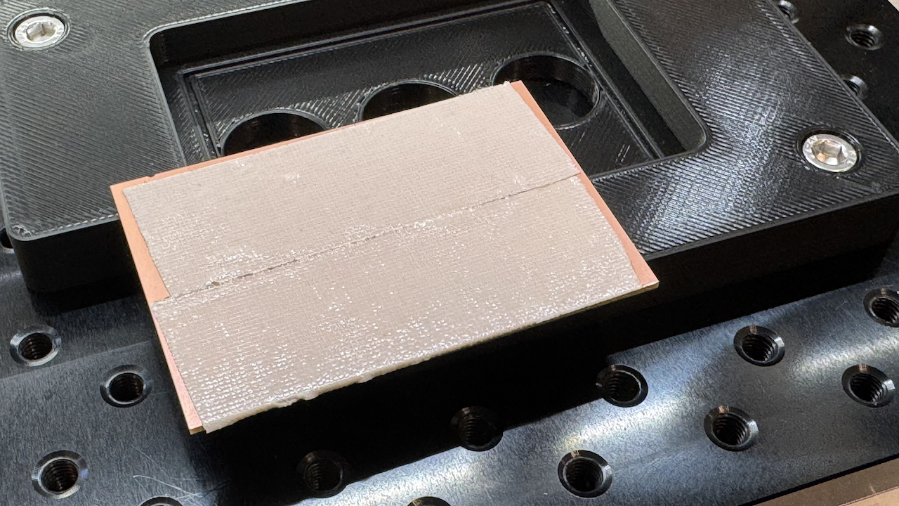
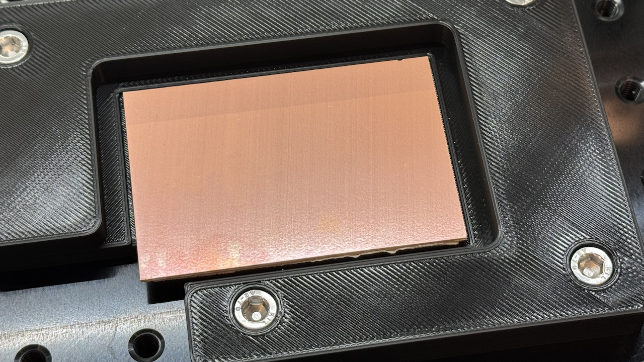
Then press the copper clad into the jig with a paper towel:
Milling with coppercli
See the coppercli README for installation instructions and full documentation.
General Notes
- As you learn, stay close to your CNC machine with your finger on the power switch.
- While learning, I destroyed half a dozen bits. Start with cheap throwaway bits.
- In the terminal, coppercli is keyboard-driven: choose menu items with the arrow keys and Enter, or with each item's letter.
- Use Jog to move the spindle. Arrow keys move X/Y, Page Up/Down moves Z. Press
Tabto cycle through speed presets (Fast/Normal/Slow/Creep).
Carbide Motion Can Fail After coppercli
Switching to coppercli after using Carbide Motion is usually OK. Using Carbide Motion after coppercli can fail, for reasons I have not found, starting with initialization and homing. Keep your finger on the power switch. If Carbide Motion misbehaves, follow my instructions to reset GRBL on a Nomad 3.
Start coppercli
Run coppercli from the command line. On first run, go to Settings → Select Machine and pick your machine (e.g., Nomad 3). This sets the tool setter position for that machine.
From the main menu, choose Connection, then Serial, and let coppercli auto-detect the serial port and baud rate. Once connected, it offers to home the machine.
If it's not working, reset the machine and restart coppercli. Make sure the door magnet is engaged.
Load the G-code
Choose Load G-Code and browse to the .ngc file generated by pcb2gcode.
Set the Zero Point
Choose Jog. Start with the Fast preset and switch to Slow or Creep as you get close.
Move the bit to the bottom left corner of the copper clad, slightly away from the alligator clip (see image below).
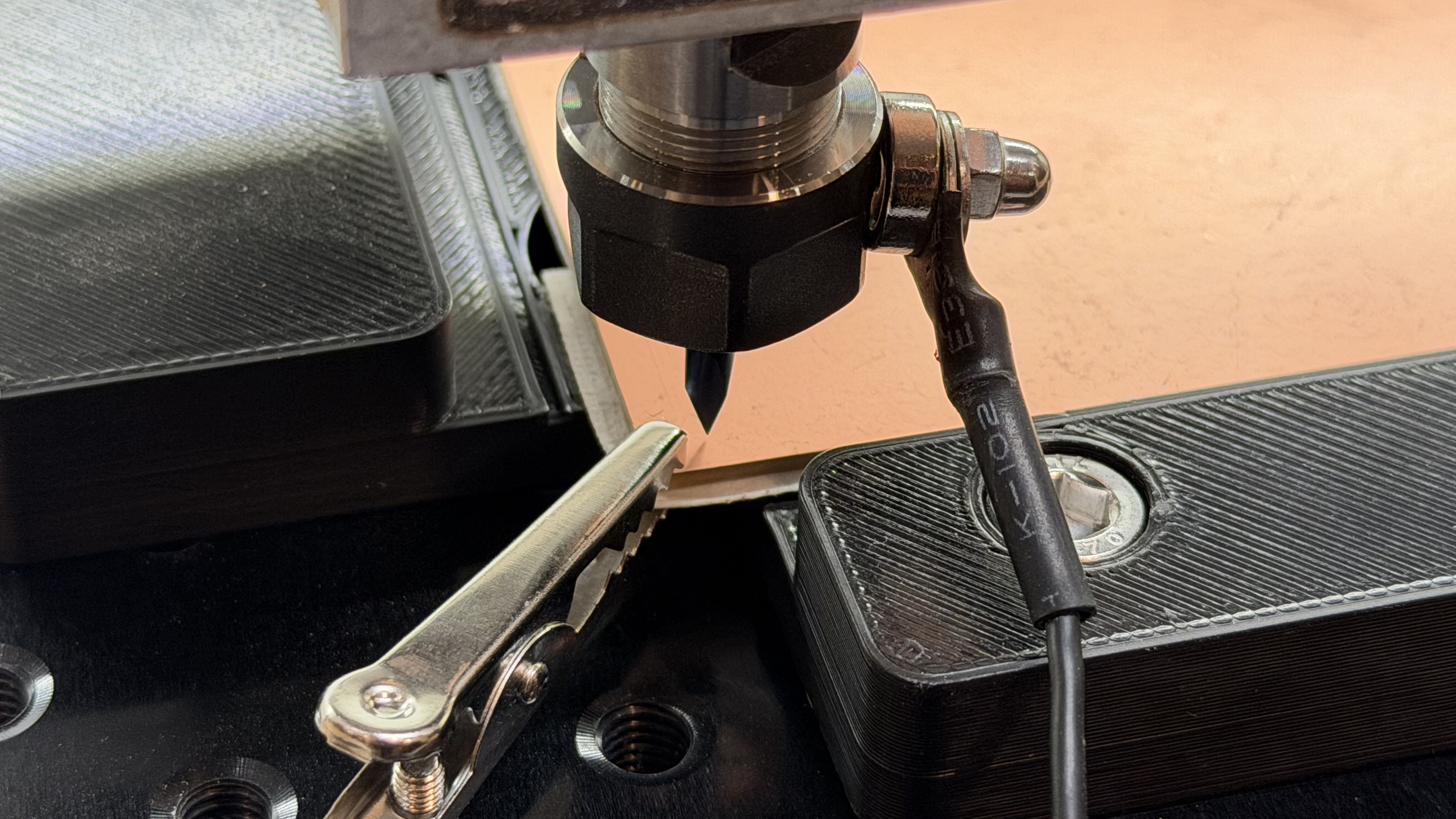
Lower the bit to about 2mm above the surface with Page Down. Then press P to Probe Z: the bit moves down until it touches the copper. In the photo below, the BitZero light has turned red, which means the bit touched the copper.
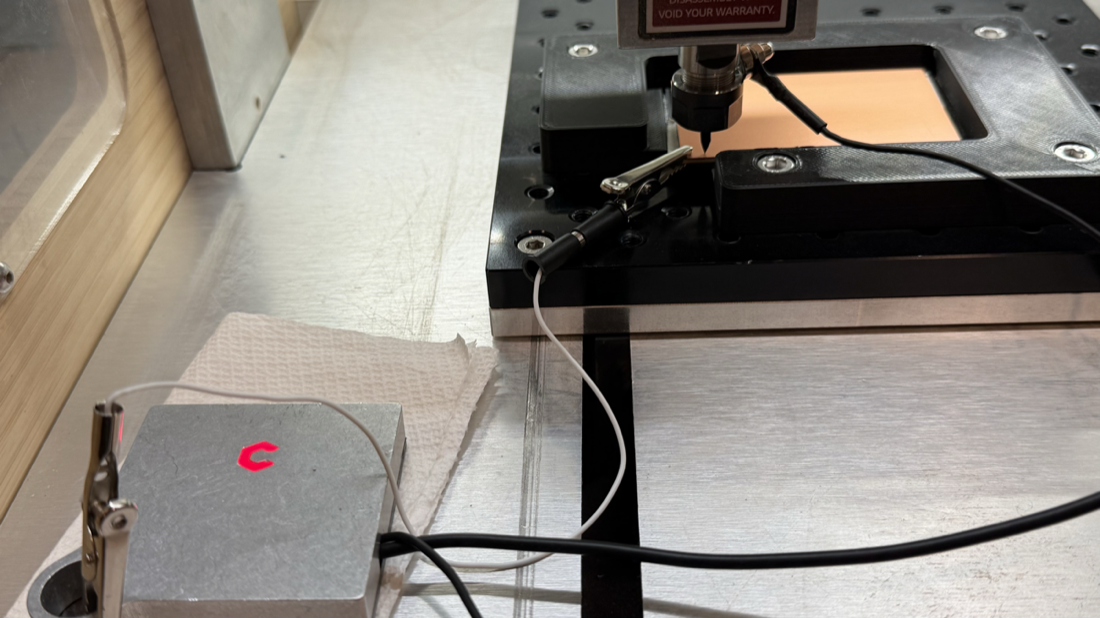
Once the probe completes, press 0 to Zero All (XYZ).
Probe the Surface
Choose Probe from the main menu. You'll be prompted to enter:
- Probe margin: Extra space around the G-code bounds (default 0.5mm).
- Grid size: Distance between probe points (default 5mm). Smaller values give more accurate height compensation but take longer.
Run Probe
Choose Start Probing. You'll be asked: Trace outline first?
If you answer yes, the bit traces the outer edge of the probe area before probing. coppercli asks for a trace height and feed rate; pick a height at which you can see whether the bit stays over the copper clad. If the bit goes past the edge of the copper, press Escape to cancel, then move your work zero before probing starts.
After the trace, coppercli probes each grid point and draws the height map as it goes: red is high, blue is low.
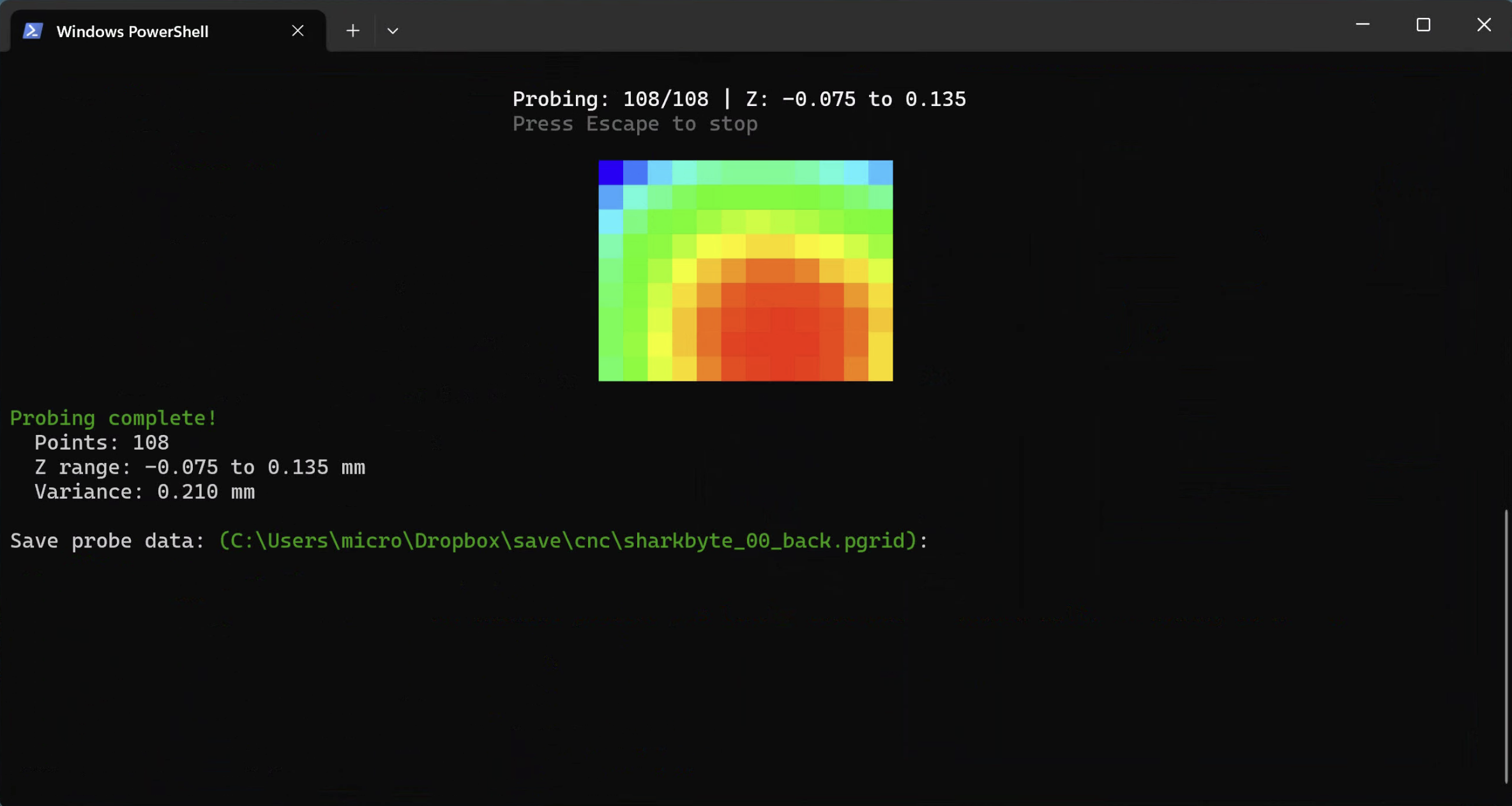
Press Escape at any time to stop. coppercli auto-saves progress, so you can resume an interrupted probe session later.
Remove the BitZero
Remove the BitZero and its alligator clip from the machine. Do not pull on the copper clad when you unclip it.
Apply Probe Data and Mill
After probing completes, coppercli will prompt you to apply the probe data to the G-code and proceed to milling. The milling screen shows progress, position, and ETA.
Before milling starts, coppercli asks whether you removed the probing equipment. On that screen, ↓ lowers the cut and ↑ raises it, 0.02mm per press. If a cut did not go through the copper, mill the board again. Lower the cut by no more than 0.1mm each time.
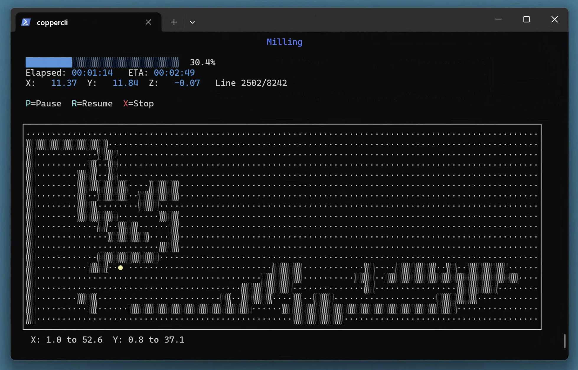
Pto pauseRto resumeEscapeto stop+/-/0to increase, decrease, or reset the feed rate to 100%
Tool Changes (milling → drilling → outline)
If you used --multi to create a single _000_all.ngc file, coppercli handles tool changes automatically. When a tool change is needed, coppercli will:
- Pause and display which tool to load
- Move to an accessible position for bit swapping
- Wait for you to change the bit and press Y to proceed
- Automatically re-zero Z using the tool setter (if configured under Settings → Select Machine)
- Resume milling with the new tool
If you don't have a tool setter configured, coppercli will prompt you to manually probe the surface with the new bit.
Flipping the Board (double-sided PCBs)
If you flip the board for double-sided milling, you must re-zero and re-probe:
- From the Jog menu, raise the bit high enough to flip the board
- Flip the board
- Attach the rigged BitZero
- Jog over the board and lower until the BitZero turns red
- Press
0to Zero All (XYZ) - Remove the rigged BitZero
- Probe again before milling: the height map from the other side does not apply
Soldering
- Sand the copper with 600+ grit sandpaper, in one direction only, not in circles. I sand right above a vacuum cleaner. Do not use 0000 steel wool: it leaves strands behind.
- Optionally, clean the surface with isopropyl alcohol using a dust-free cloth.
- Stick the pin headers or components through the holes.
- Dab the tips and copper with a flux pen. Don't worry about the board absorbing flux.
- Use magnifying glasses.
- Use the finest soldering tip.
- Use very thin (lead-based) flux core solder.
- Solder the pins to the copper pads; use as little solder as possible.